News Centerbarrow
Industry News
Intel has released the largest FPGA at present -- Stratix 10 GX 10M with 43.3 billion transistors on a single chip
2019-11-07 10:58 The author:Administrator
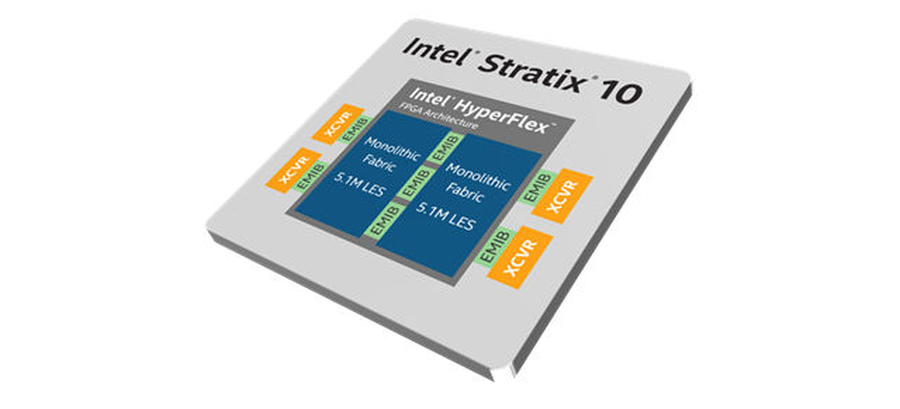
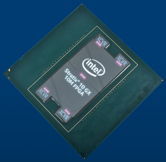
Intel recently announced the world's largest FPGA chip, Stratix 10 GX 10M, which integrates 43.3 billion transistors at 14nm. While achieving this record, it also USES Intel's newer EMIB technology to connect the two FPGA cores.

FPGA is like a piece of plasticine, and engineers can program FPGA with hardware description language to enable it to execute specific programs. Compared to complex cpus, it is much easier for fpgas to achieve larger scale with the same process, such as the Virtex UltraScale+ VU19P FPGA launched by cylins in August, which has 35 billion transistors.

This is from Tom's Hardware
Intel's FPGA actually contains two identical FPGA cores, with a total core area of 1400mm^2^ and a transistor density of 31MTr^2^. The two FPGA cores are interconnected with Intel's new EMIB technology, with a data bandwidth of up to 6.5TB/s, and EMIB is also used to connect FGPA to peripheral silicon chips. This is actually the first time that Intel has used EMIB technology between these two huge silicon wafers. Previously, EMIB played the role of an Internet channel between Vega GPU and HBM memory on Kaby lake-g, with a much smaller bandwidth than EMIB channel on Stratix 10 GX 10M.
At present, FPGA is widely used in ASIC design, and the market pursuit is that the more programmable logic units the chip provides, the better. Therefore, several large FPGA manufacturers have been committed to introducing larger and larger FPGA chips. The Stratix 10 GX 10M has 10.2 million logical units, 1.2 million more than the 35 billion transistors integrated Virtex UltraScale+ VU19P FPGA, and nearly four times as many as the Stratix 10 GX 2800 before the Stratix 10 GX 10M. The interconnection technology used in the new FPGA also represents the future development direction of Intel chip packaging technology -- multi-silicon chip packaging, connected by EMIB and other interconnection technologies.
Article reproduced from: super power network

